I had the pleasure to attend the SEMI event held November 2nd in Beaverton, Oregon, just a few miles away from where I live in Tualatin. Biamp hosted the meeting, and their company has been in the area for 50 years now, providing professional AV equipment. They even had a free app to turn your smartphone into a microphone during the Q&A session, something that I’ve never seen before.
Martin Dixon from Google Cloud presented first on the topic, Open Chiplets to Enable a New Era of Silicon. The demand for compute, especially for neural network needs are exponential. On the YouTube platform there are 100’s of hours uploaded per minute, and about 54% of Internet traffic is video. The power efficiency of servers is slowing down, while the cost/byte has plateaued for disk storage.
Clearly there is a need for accelerators, so the Google Video Coding Unit, announced in 2021, is an SoC to transcode video streams – change formats for screen sizes and size. The VCU provides the best compression engine, smallest video sizes, and enable video transfer in the quickest time. With a 5 second clip it takes 15 minutes of CPU time to transcode on a general purpose CPU, but with the VCU is 30X faster than a CPU.
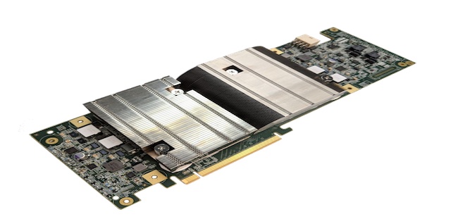
For Machine Learning (ML) acceleration, the Google TPU v1 came out in 2015 to accelerate inferencing, and it’s a co-processor working next to a CPU. As a single-chip system it provided 92T Ops/sec operating at 700MHz.
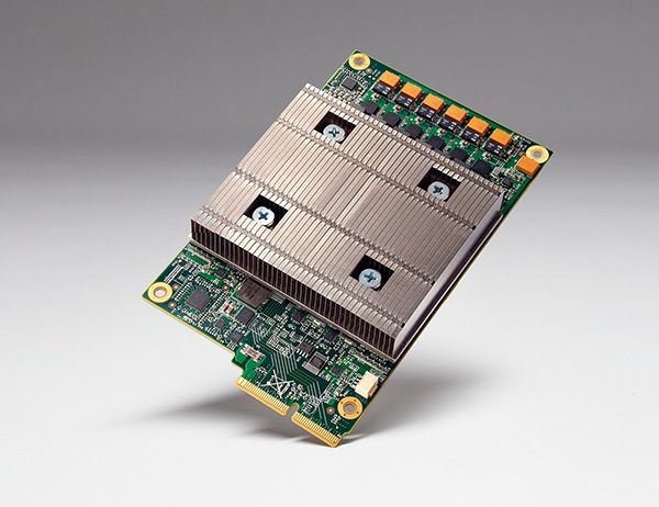
The next generations of accelerated training for learning were the TPU v2 in 2017 (180 teraflops), and TPU v3 in 2018 (420 teraflops). Combining TPUs into pods brought the performance up to 11.5 petaflops and 100+ petaflops, respectively.
TPU performance was impressive, however custom silicon is expensive to design, manufacture and deploy, plus the reticle limited die sizes for the TPU v2 and v3 and there were poor yields. At TSMC a 300mm wafer at 5nm is priced at $17,000, and to get 100 good chips per 300mm wafer it costs about $170/chip before packaging.
So chiplets are one way to get better costs, recent AMD and Intel GPU and CPUs are early examples of Chiplets, as they allow you to bo beyond the maximum reticle limit per architecture. Chiplets can also reduce device design time and costs. Smaller die improves silicon yield, and with chiplets you can use different process nodes per system function: logic, memory, IO, analog.
Two prominent chiplet examples are the AMD EPYC 7002 (Server chip), Intel Lakefield.
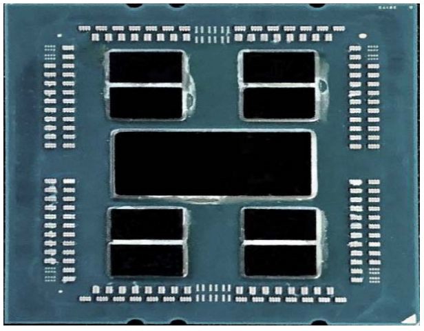
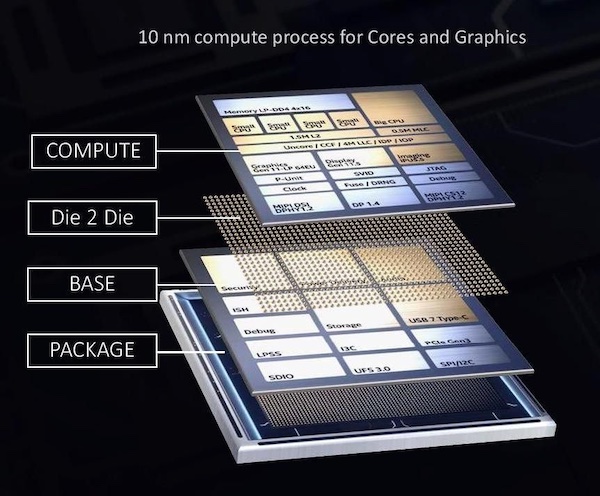
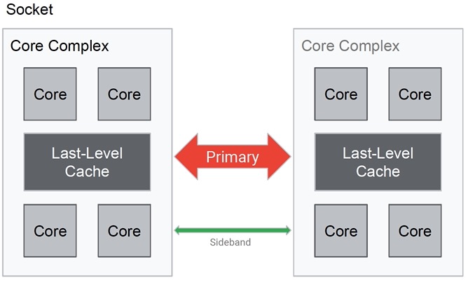
A good chiplet example would be for Non-Uniform Memory Access (NUMA), where a 16 core machine with shared cache is broken into Chiplets, while any penalties for crossing chiplet boundaries could be addressed by partitioning.
With a chiplet-based approach, there are questions surrounding both security and manageability, primarily at the interface between Chiplets. Sideband has security and manageability, but how do you trust adjacent chiplet data? Is the chiplet next to me powered on?
Also from Google Cloud was Amber Huffman, talking about using standard form factors for chiplets. There are plenty of emerging standards: AIB, USR/XSR (older), Open HBI (Open Compute Project), BOW, UCIe (March 2022). UCIe brings in the PCIe and CXL protocols, where we want to build up the entire stack. The SoC with chiplets is the new motherboard, just like the previous ecosystem placed components onto boards, so we have a dream of lego-like assembly.
AMD and Intel cannot share Chiplets today, because of their divergent approaches, so how do we as an industry make Chiplets a plug and play problem?
The third speaker was Farhana Sheikh, Ph.D. from Intel, presenting, New Era of Circuits, Systems and Heterogeneous Integration. There’s been a trend for convergence of intelligence, compute and communications. The number of connected devices is predicted to be 500B by 2030, which is 59X larger than the world population.
Technologies creating all of these connected devices include: AR/VR, machine to machine connectivity, imaging, sensing. Electronic objects will fill up all of the communication channels with data, so we need AI/ML to improve system performance to handle this new wave of data, and with 6G limits we reach 1 Terabit speeds.
Way back in 1965 Gordon Moore formulated his famous scaling laws, yet also introduced the concept of heterogeneous integration and co-packaging. An early chiplet at Intel was combing FPGA, foundry IO chiplets and HBM, announced in 2019. A 3D integration approached called Foveros combined FPGA and memory by placing
Intel has supported both the Advanced Interface Bus (AIB) version 1 and 2, as a high-density die to die interconnect. In 2017 Intel showed their EMIB technology to connect an FPGA die with transceivers.
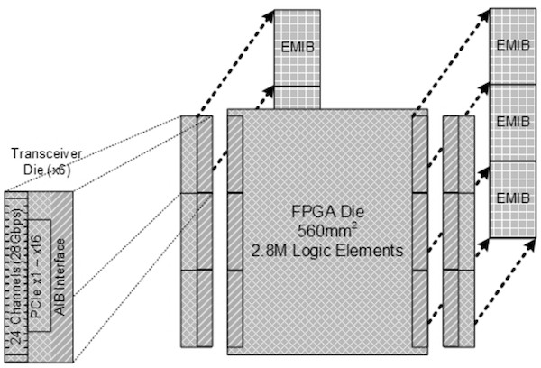
DARPA did a Heterogeneous Integration project combining an Intel Stratix 10 FPGA with ML/AI chiplets using a 55um EMIB, having four 16×16 systolic arrays, producing 6.97 TFLOPS/W. Another DARPA project combined optical chiplets and FPGAs using the AIB 1.0 spec, presented at HotChips 2019.
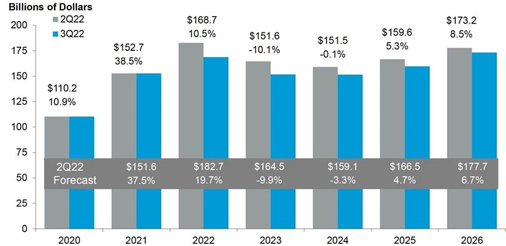
After a 15 minute break, there was Bob Johnson from Gartner taking us through a Q3 22 Semiconductor Market Outlook. There’s market weakness in memory, while some strength in non-memory segments, so the semiconductor forecast is:
- 2023, -2.5%
- 2024, -6.9%
- 2025, 8.6%
- 2026, 8.2%
Both the consumer and enterprise markets are following similar cyclical patterns.
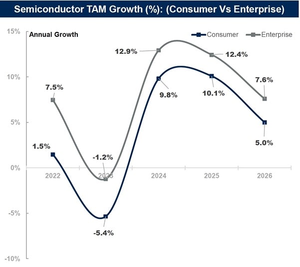
Smartphone production is forecast to bottom in 2023, then return to 6.2% growth in 2024. There was a COVID-induced peak for 2021 in PC production, but it fell in 2022 and will bottom in 2023 also. Automotive and Industrial drive analog, discrete and MCU growth, yet there is still automotive chip shortages (Toyota, etc.)
Bob’s summary forecast is down for short term outlook, inventories will eventually return to normal levels, while lead times to shorten in devices and equipment markets
The Capex outlook predicts declines in 2023, although it was up 7% in 2022 (down from a 19.7% forecast).
The CHIPS act has both grants and tax credits that expire in 2026, and the focus is for total semiconductor research infrastructure like University, Defense department, NSF and education in schools. Plenty of fab expansion plans in the USA from: TSMC, Intel, Samsung, TI, Micron, SkyWater, GlobalFoundries.
Recent China export restrictions are directed at advanced AI and supercomputing limitations, with some exceptions for Samsung, SK Hynix, TSMC. There are 31 companies on the Unverified List, including YMTC, so the Chinese memory companies are impacted.
In summary, our semiconductor industry is in a pause phase, and this is yet another cyclical downturn like many before it.
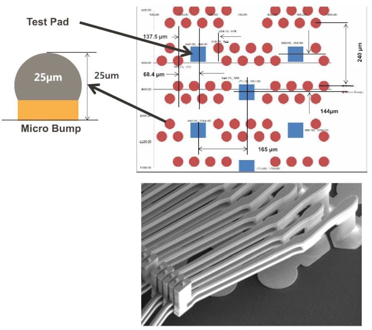
Amy Leong from FormFactor was up next, and her company provides wafer probe equipment used to test die on the wafer and chiplets. Probe card spending as a percentage of semiconductor revenues ranges between ~0.35% to 0.4%, and Form Factor is number one in this market, with 2,300 employees and $760M in revenues.
Probe cards have followed package pitch at about 400 microns, down to 150 microns on flip-chip, and 80 microns for copper pillar, then requiring 40-10 microns for Chiplets. Wafer tests for performance decide which chiplets should be used. By 2030 the forecast is that chiplets with 10um pitch will be using hybrid bonding technology.
One challenge for probe cards is meeting the current carrying requirements as pitch gets smaller. A hybrid probe card uses a layout of power and ground interconnects at larger pitches, while the remaining pitches can be higher density and fine-pitch with lower currents.
Micro-bumps are used for high-volume HBM manufacturing, and one HBM stack used 8 RAM die and one SoC die. The red bumps are for HBM at fine pitch, while the blue pads are set at larger pitches.
Packaging techniques help extend Moore’s Law, as assembly and test become more important drivers, so expect spending or probe cards to increase as challenges are met for higher currents, smaller pitches and finding Known Good Die (KGD).
Our final speaker was Mark Gerber, from ASE Group, sharing on Advanced Packaging.
this is the most exciting time in packaging ever
From 2020 to 2021 we had the early COVID work from home years, which then showed a broken supply chain, impacting many products with chip shortages required for cars. With these supply chain challenges there is the rise of on-shoring, and a growing of fab capacity to match demand.
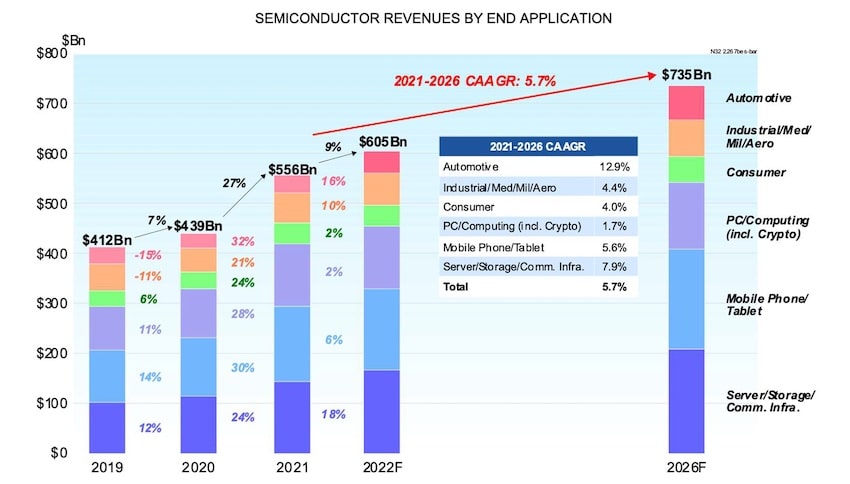
Semiconductor revenue predictions from 2022-2026 show a 5.7% CAGR in six product applications.
Chiplets are attractive for lower costs and higher yields, but then chiplet integration requires advanced packaging, so packages are sexy again. The costs of silicon development are only getting higher: 28nm at $45 million, 7nm at $210 million, 5nm at $400 million, 3nm at $497 million, and 2nm at $634 million. IO bandwidth has been doubling every 3 years, there is higher power consumption and silicon density scaling is tapering out.
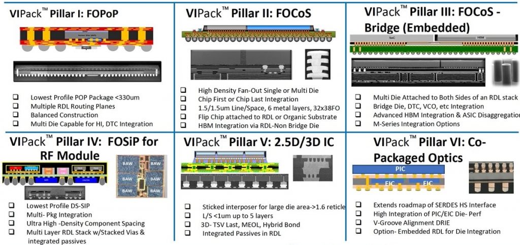
Chiplets will be used in AI/ML, network switches, servers with GPU and CPU, plus PCs. ASE Group has technology called Vertically Integrated Package Platform – VIPack, announced June 1, 2022, which has six configurations:
- Fanout Package on Package, FOPoP
- Fanout Chip on Substrate, FOCoS
- Fanout Chip on Substrate – Bridge, FOCoS – Bridge
- Fanout System in Package
- Pillar V: 2.5D/3D IC
- Pillar VI: Co-Packaged Optics
There are new ecosystem opportunities as Moore’s Law has slowed down, so disaggregated approaches using chiplets is a means to control costs and maximize yields. Both OSATs and foundries are shifting their CapEx into advanced package technologies to meet these opportunities.
Summary
The quality of speakers and timeliness of the chiplet topic were a big draw for me and others who attended this live event. It was implied that EDA vendors are enabling this transition from SoC to the chiplet world, as electronic design automation tools ensure that chiplets are tested properly, predict the power required, keep the temperatures in spec, and verify that all of the interconnects are valid and that silicon will be reliable.
SEMI provides an archive of the event on their site, and I look forward to their next event in Oregon.

