
- This event has passed.
Keysight EDA Connect World Tour: Santa Clara – High Speed Digital
February 28, 2024 @ 9:30 am - 3:15 pm PST
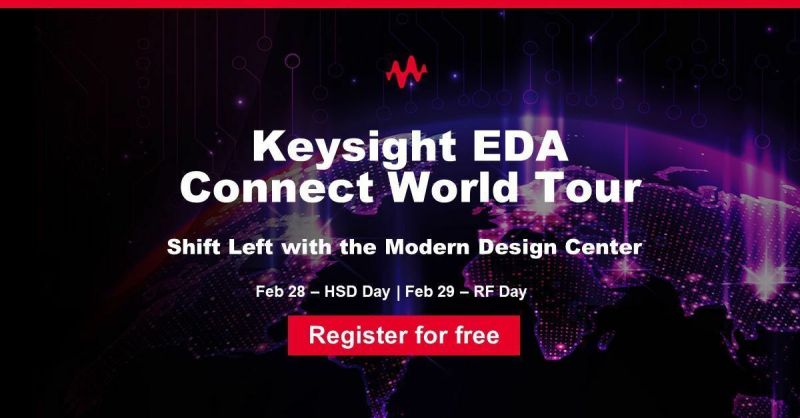
Shift Left with the Modern Design Center
Artificial intelligence (AI) is redefining high-speed digital designs. Your ability to design, simulate, and test — using an automated, integrated workflow — is what will set you apart.
Whether you are a design team leader, digital designer, or system engineer, this one-day event is for you. We have assembled speakers and sessions for every skill level to take your company and career to the new frontier. Sign up now to do the following:
- Learn and experience advanced digital design solutions, including die-to-die simulation for chiplets, SerDes and memory design for AI/ML, and more.
- Gain practical insights from case studies presented by local customers.
- Connect with peers and technical experts at the heart of the Silicon Valley.
Register now to secure your seat.
| Agenda | High Speed Digital Focused |
| 09:30 – 10:00 | Check-in |
| 10:00 – 10:10 | Welcome/Keynote |
| 10:10 – 10:45 | Chiplet PHY Designer- Analyze D2D to D2D |
| 10:45 – 11:30 | Advances in memory and SerDes applications |
| 11:30 – 12:30 | Simulation-driven compliance solutions for PCIe and USB standards |
| 12:30 – 1:30 | Lunch Break – Keysight Design Data and IP Management |
| 1:30 – 2:15 | EM modeling of high-speed interconnects using SIPro |
| 2:15 – 3:00 | End-to-End Power Integrity Simulations with Digital Twin EM Models |
| 3:00 – 3:15 | Closing remarks / Survey |