In SoC designs today parasitic extraction tools produce RC and sometimes L or S-parameter values for full-chip designs using either pattern-matching or equation-based techniques. It gets the job done for most digital designs however when you really need accuracy in your parasitics then you must consider something more accurate, namely a 3D field solver.


Most 3D field solvers are slow (compared to pattern-matching) and quickly consume RAM which then limits the practical capacity to cells or small blocks.

Silicon Frontline saw this opportunity and announced products earlier this year to address 3D extraction (F3D) and 3D resistance for power devices (R3D). I spoke today with Dermott Lynch of Silicon Frontline to get an update since August 2009.

Canesta sees value in using F3D for their line of 3D image sensors. It saves them time from having to build a test chip and make measurements, now they can simulate with confidence.

Aptina is a second image sensor design company using the F3D tool to shave 4 months off their product schedules using simulation with accurate parasitics.
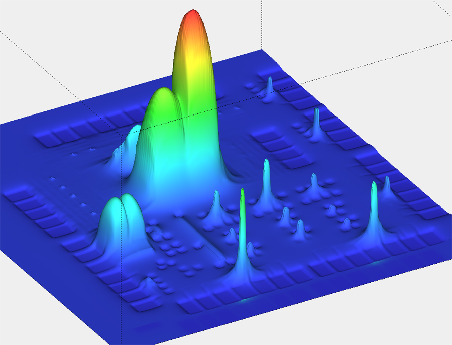
Designs requiring this high accuracy include: SRAM, DRAM, Flash, image sensors, ADC.
In evaluations there is always the question of a reference for accuracy comparisons so the venerable QuickCap and Raphael tools are often used. F3D compares well with these reference tools then really shines when you turn on the manufacturing effects.
In 2010 you can expect to see:
- Endorsements from foundries
- Speed improvements
- Two new products
This EDA company has found a niche in offering fast and accurate 3D extraction and a growing list of customers.


Another happy user named Triune Systems