Digital designers are taught on day one that they must use synchronous logic design which employ a clock to synchronize all events in their IC design, and so it has been for decades.
Unless of course you have ever designed a DRAM or SRAM memory where self-timed logic is used to squeeze out the ultimate in performance. I started out designing DRAM circuits at Intel (when they were still in the DRAM business) and was delighted to learn that my chip was using self-timed logic to increase performance and simplify the interface requirements when the memory was placed on a board.
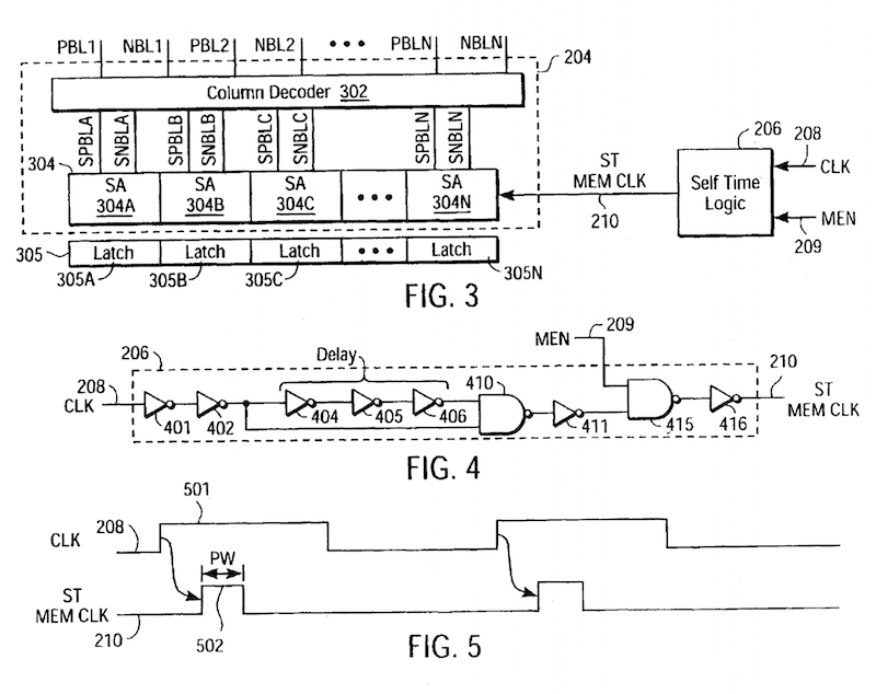
Self-timed logic for Memory, Patent 6785184 (Intel)
What would happen if you could design your digital logic without the use of clocks?
Indeed, you could benefit by:
- Faster operation
- Process variation tolerance, delay insenstive
- Lower power (no clocks)
- Low current peaks
- Operate over a wider voltage range
- Lower latency
- Quicker wake-up times

I recently met with Steve Svoboda from Tiempo IC, a company offering IP and EDA tools for clockless design.

Q: What is your history in EDA?
A: I worked at Alta which was bought by Cadence in 1995 and was the product line manager for SPW. I used Alta at GTE then joined Alta. Cadence also bought Redwood Design Automation and the product lines merged and were called the Alta Group.
Q: What is the mission of Tiempo IC?
A: To raise the abstraction of self-timed IC design from the transistor level to the RTL.
Q: Who founded the company?
A: Marc Renaudin, former Professor at Grenoble INP did research in asyncrhonous logic as applied to crypto processor design along with logic synthesis.
Q: How does asynchronous logic work?
A: In between logic stages there’s an asynchronous register (Muller Gate, C-Element), then combine that with dual-rail encoding of data (provide delay insensitive design). An acknowledgment is sent back that data was received, then it’s ready to send the next data.
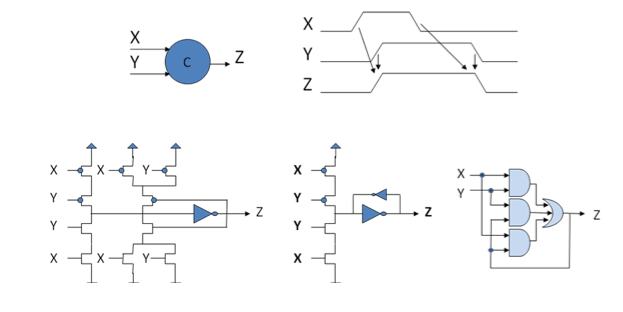
C-element, Muller gate

Four-phase communication protocol
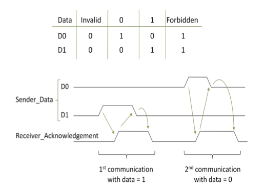
Dual Rail Encoding
Q: How does the asynchronous approach differ from synchronous logic?
A: In synchronous logic your design is limited by the slowest path, and this design style creates current spikes at each edge of the clock.
Q: With synchronous logic I have a well-founded test plan. How do I test a clockless design?
A: Asynchronous is not testable in the same way that synchronous design is. On the plus side we don’t have race conditions or glitches to contend with. Our testability problem is really combinational logic instead of sequential logic, which means a huge reduction in the number of logic states.
Q: Is there any ATPG with asynchronous logic?
A: Stay tuned for more info.
Q: How testable would a CPU be in clockless design?
A: We built and tested a 16 bit CPU which required only 420 vectors to test, compared to traditional sequential designs which would require thousands of vectors to test.
Q: What is the input language for your EDA design flow?
A: Our tool accepts SystemVerilog.
Q: Who else has designed clockless chips?
A: Handshake Solutions did an ARM core for Philips that was clockless.
A: Achronix is an FPGA company with asynchronous design and their parts run at 1.5GHz rates.
A. Fulcrum Microsystems offer switches that are asynchronous providing the lowest latency in the market plus lower power.
Q: What are the big benefits of using clockless design?
A: Lower power and delay insensitive designs.
Q: What does Tiempo IC offer today?
A: Both IP cores and EDA tools for asynchronous designs.
Q: Can you mention any customer names yet?
A: No, we are under NDA and the customers are not allowing us to talk about them yet.
Q: Can I run a Static Timing Analysis (STA) tool on your asynch designs?
A: Yes, any commercial STA tool will work on our designs.
Q: For your synthesis tool, what is the capacity?
A: We have not yet tried to measure the capacity of ACC. But we routinely synthesize blocks of around 500k gates, and have successfully synthesized designs up to 5M gates.
Summary
Asynchronous logic design has been around a long time, and now we see Tiempo IC bringing their own IP, services and EDA tools to a larger audience by using SystemVerilog as an input language.


Interesting!
How does this fit into overall SoC/chip-level integration where different kinds of IP will need to be brought together? Also, how about tools interoperability with other EDA tools?
Rahul,
You could place your clock-less block anywhere inside of a traditional SOC. STA will run OK on the clock-less block, however you cannot run ATPG on the clock-less block.
The input to the Tiempo tools is standard System Verilog, so that would fit into your flow.
What we really need to see is a white paper from one of the Tiempo customers to show us in detail how they made all the EDA tools work together.
The question from Rahul open a new field: if a customer wants to get the benefits from asynchronous design, but still use existing (synchronous) IP, then why not proposing to transform these IP into async. functions?
Would this be a viable business model for Tiempo? There could be a strong demand coming from the portable industry, if the benefits in term of power consumption are large enough…
Eric,
Exactly right, Tiempo IC does offer design services and will convert your existing synchronous design into an asynchronous one.