On Thursday morning I spoke with Dian Yang, Sr VP of Product Engineering at Apache by phone about a new ESD software tool called PathFinder (sorry Nissan, but this isn’t an autom0bile).
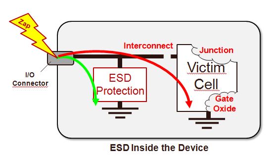
I learned how ESD can destroy an IC both during packaging or when placed in the system:
Just like a lightning rod grounds a high voltage strike, ESD protection creates a path to drain the current or charge before it hurts the rest of the IC.
Voltage inputs can exceed 8,000 volts. In the old days you could test 20 – 100 devices as a sampling (IEEE mil standard). Every pin would need to be tested. On a 1,000+ IO pads would then create 1,000,000 pair combinations, which is simply too large of a number to test quickly or economically.
Instead of only relying on physical testing the new PathFinder tool uses SW to simulate ESD and pinpoint the weak points in your IC design.
This new tool can test all 1,000,000 pin pair combinations in just a few hours for most IC designs.
The chip itself can build up a charge during assembly, creating a static charge, during assembly the chip touches the board and discharges current (most important now during assembly). Biggest yield loss, can be 20 to 30%.
The ESD zap can create opens in metal through electro-migration.
Voltage islands for multiple power domains also use ESD devices for protection. How do you test each power domain?
ESD protection doesn’t really scale down. 65nm ESD protection device is 250um on a side. If you leave out ESD devices to save area then you are simply risking your IC design.
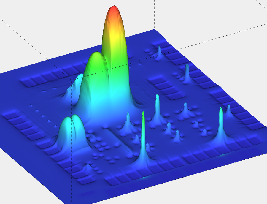
PathFinder can check each power domain for ESD, and even the combinations between power domains. Each zap shows you the current density (Gate Oxide, Melted vias). At the full chip PathFinder use a switch level model.
For block level ESD analysis is dynamic, each device uses BSIM4 like models. The idea is to measure, analyze then pinpoint ESD failures. A block with 100K transistors will simulate over night using dynamic simulation.
One technical challenge is how to model transistors up to 2,000 volts for IV curves. This is quite different modeling because it includes an effect called snap-back. The foundry provides some info on high voltage operation. Snap back looks like negative resistance, so Newton Raphson simulation techniques cannot converge. Apache uses a new simulator called eSIM that handles negative resistance during snap back.
The IC substrate is part of the discharge path for currents, so you need to model the substrate.
The PathFinder engine uses a multi core linear solver and can also be used with cloud computing.
The pricing for PathFinder is $180K annually and is an option on top of Red Hawk (SOC) or Totem (Analog). A 4 core CPU is good enough to simulate most ICs and it’s typical to use 64GB of RAM.
You would use PathFinder as a sign-off step for each IC design. The tool could even be run early in the design process for prevention purposes, so it could be run 10 times per design.
Summary
Apache has created a new tool category for ESD simulation of both blocks and full chip. As the first entrant they can command a high price tag, so expect to see competition emerge in the next year or two from the big four in EDA or maybe even a new start-up.


Hi Daniel,
Interesting. ESD is such a “black art” that it would be good to have tools to predict performance. Hopefully this works pretty well.
I have 2 questions:
1) Do any other vendors have similar tools for ESD simulation? I recall there might have been a small company called Lynguent that played in a a similar space.
2) You mention that Pathfinder “can be used with cloud computing.” What does that mean? Has it been proven out on a particular cloud provider? Is it available on the cloud?
Harry,
1) I know of no other EDA tools in this category.
2) Cloud computing to mean a compute farm (I think, but will double check.)
Hi Daniel,
I just wanted to let you know that customers do have a choice when it comes to tools that check IC designs for protection against ESD. In fact, Mentor Graphics Calibre PERC (programmable electrical rule checker) has been in production use at multiple customers since last year. It was also selected by the editors of Electronic Products magazine for their Product of the Year Award in 2009 (http://bit.ly/5V5pKT). For information on Calibre PERC, see http://bit.ly/d1SJBR, or follow product links from http://www.mentor.com.
Gene Forte
Mentor Graphics
Gene,
Thanks for the info, however PathFinder actually runs a simulation and pinpoints ESD hotspots in the IC layout.
When I read what Calibre PERC does it is not an Apples to Apples comparison with PathFinder because PERC is not performing any simulation, it is only running ESD layout rule checking.
Your group should have a talk with the ADiT or Eldo circuit simulation group to come up with a competitive response to PathFinder.
BTW, Calibre PERC is supported as the ESD checking solution by ISDA (International Semiconductor Development Alliance–the technology alliance between IBM, AMD/GlobalFoundries, Freescale, Infineon, NEC, Samsung, STMicroelectronics and Toshiba).
Gene,
Thanks for the info on customer adoption, PERC looks quite useful.
Do you agree that PERC and PathFinder are still different types of ESD tools?
FYI – Engineers from Infineon presented at DAC on ESD issues and EDA tools, both layout-based and simulation-based. http://www.slidefinder.net/1/12_4/325856
Daniel-
Regarding your question to Gene, yes we agree that Pathfinder and Calibre PERC are different types of tools.
With PERC, while we are leveraging one of our strengths which is (layout and circuit) verification, we also have incorporated simulation capabilities to address the types of problems you discuss above.
Also, PERC is used in other areas (outside of ESD) as well. When you have the time, I would like to provide a more complete description for you to make your own assessment.
thanks
Carey Robertson
Mentor Graphics Corporation