Who
Jerome Toublanc, Principal Product Engineer at Apache Design Automation

Overview
Notes
PathFinder – ESD integrity for advanced electronic circuits
What is ESD?
ESD for an IC at an IO pad. How do you protect your IC layout?
Failure – breakdown of interconnect, junction or gate oxide.
Protection – ESD protection, clamp cell. Make the discharge go through a known path. Placement of ESD cell is critical for safety.
History – At 180nm device channel heating during ESD discharge, at 65nm will gate oxide break, at 32nm and lower what is metal reliability?
Metal Reliability – amps per cross area. At smaller nodes the lifespan can decrease.
Three ESD models – Human Body Model (HBM), Machine Model (MM), Charged Device Model (CDM). Different classes per model: HBM Class 0 thru 3B, MM class M1 thru M4, CDM Class C1 thru C7.
Goals – perform ESD analysis early before tape-out, optimize my circuit, predict failures, minize overdesign
Approaches – engineering guidelines, visual plot checks, ERC (circuit netlist verification)
PathFinder Inputs – uses layout, technology plus rules.
Outputs – Pass/fail checks for HBM, MM, CDM
Layout based analysis:
– HBM/MM – bump2bump, bump2clamp
- Example: 18 million instances, 702 power pads, 38 power domains, 2.5 hours run time
- Resistance network for VDD/VSS has to be extracted (same extraction engine as other Apache tools)
– CDM – static, dynamic
– EM – current density checks
Totem (block level, transistor level) or Redhawk (full chip) tools – can call PathFinder
Layout Based Analysis and Debug – IC layout that can be clicked on, see the ESD rule check results, display of the ESD path highlighted.
CDM Event Modeling – path between the die and the clamps. Tool has to compute all paths between VDD and VSS. Is the loop resistance below my threshold? Idenitfy logic cell to clamp cell discharge paths, compute arc resistance, compute loop resistance.
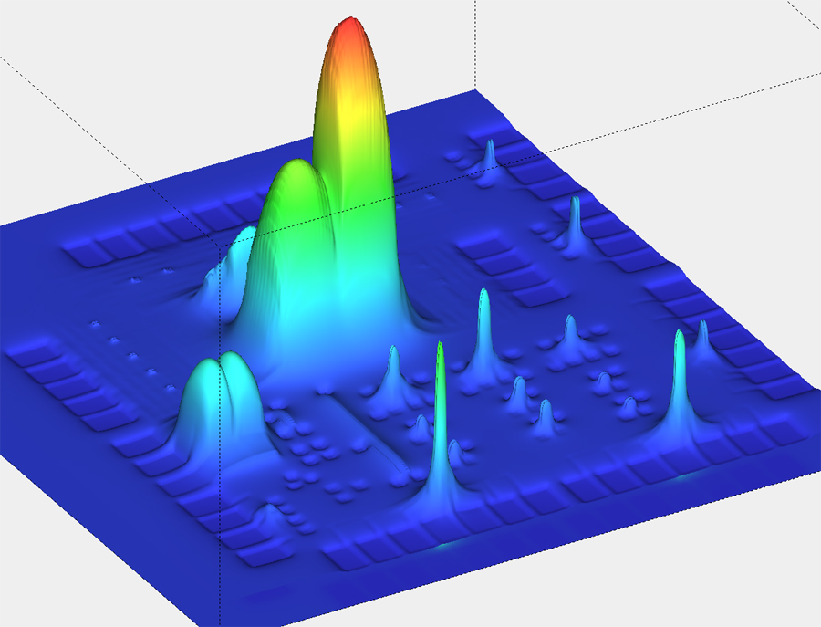
Current Density Check for ESD Events – Current density plot, EM plot. Highlights any rule violations so that you can go back and fix the nets.
– Example: 17.35M, Nodes 133.85M, #clamp instance, 83, 5 hour run time, 54GB of RAM needed.
Transient Simulation based sign-off validation for CDM
– Built-in extraction engine (on die RLC, package RLCK/S-param, include substrate RC network)
– Proprietary modeling methodology
– High voltage modeling
– Clamp snap-back profile
– SPICE accurate simulation technology (propriety simulation engine, transistor level capacitance modeling)
– Layout based debugging GUI (cross probing, what if analysis, devices failure reporting)
– Today the have a transistor level flow. A higher capacity cell-level flow is under construction.
Analysis Flow – setup and load design
– Extract PG RLC, substrate network
– Connect package netlist
– Perform simulation
– See the discharge voltage as a function of time
Prediction of ESD layout needs – how to do early planning and prototyping?
- Define your floor plan
- Predict block capacitance (CDM)
- Define your PG grid
- Define the PG pads
- Explore clamp placement
- Verify current density limits (visual rainbow plot on the layout)
Conclusions
PathFinder – ESD verification for early and sign-off design stages
- Prediction of ESD protection needs
- Full-chip multi-domain analysis capability
Q: how does the Calibre PERC approach compare to this?
A: not really sure of their capabilities.
Q: If you are testing Pad to Clamp and the Clamp has many fingers, do you handle that?
A: Yes, we do.
Q: Any correlation between your analysis and silicon measurements?
A: It’s kind of early to say. MoSys wrote a paper, “Reliability and mitigation of ESD induced failures for Advanced IP Designs”
Q: Any use of multi-core?
A: Yes, during some of the simulation can use mult-core.
Q: Any convergence issues?
A: Some early on but all resolved.
Q: What are the simulation result outputs?
A: Currents plotted graphically and numerically. Probe the current and voltage along any path.
Q: Do you support inductors in the modeling?
A: Yes, we simulate inductors for dynamic.

[…] ESD integrity […]