-
-

Optimal circuit sizing strategies for performance, low power, and high yield of analog and full custom IP
There have always been good reasons to port designs to new foundries or processes. These reasons have included reusing IP in new projects, moving an entire design to a smaller node to improve PPA, or second sourcing manufacturing. While there can be many potential business motivations for any of the above, in today’s environment with… Optimal circuit sizing strategies for performance, low power, and high yield of analog and full custom IP
-

How to Sign Off a 10 Billion+ Transistor Design in the Cloud
Advanced semiconductor applications such as artificial intelligence / machine learning (AI/ML) and graphic processing units (GPUs) fully leverage dense, advanced-node technology to push the extreme limits of design size. To signoff such large designs, engineers are increasingly relying on distributed compute methods to accelerate the signoff analysis. Furthermore, given lack of scalability of on-premises compute… How to Sign Off a 10 Billion+ Transistor Design in the Cloud
-
LIVE WEBINAR: How to Simplify the Verification of Bus Interfaces (US)
Abstract: Today’s FPGAs and SoC FPGAs use various types of bus interconnect - such as AXI, APB, AHB, Avalon or Wishbone - for both internal (IP-level) and external communication. A recently added feature to Aldec’s ALINT-PRO allows designers to extract, review and verify the correctness of bus interface connections. In addition, ALINT-PRO is capable of… LIVE WEBINAR: How to Simplify the Verification of Bus Interfaces (US)
-
58th Design Automation Conference
Moscone Center 747 Howard Street, San Francisco, CA, United StatesThe Design Automation Conference (DAC) is the premier event devoted to the design and design automation of electronic systems and circuits. DAC focuses on the latest methodologies and technology advancements in electronic design. The 58th DAC will bring together researchers, designers, practitioners, tool developers, students and vendors.
-
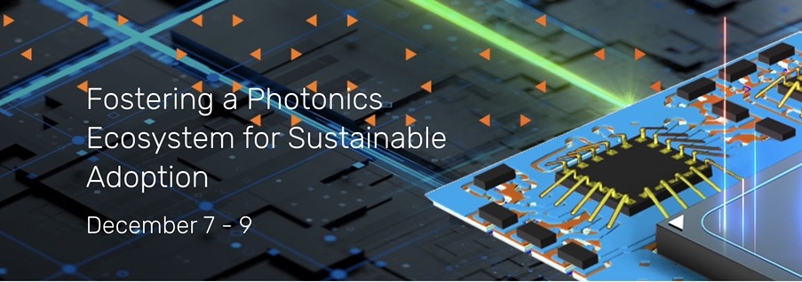
Fostering a Photonics Ecosystem for Sustainable Adoption
Integrated photonics adoption has made tremendous progress but is still slow and uneven outside of its most common use in data communications. What will it take for photonics to become a “standard” technology in the toolbox of system designers? Join Cadence for the sixth-annual CadenceCONNECT Photonics event on December 7 – 9 to find out… Fostering a Photonics Ecosystem for Sustainable Adoption
-
SEMICON West
Moscone Center 747 Howard Street, San Francisco, CA, United StatesYour Health & Safety is our first priority— Proof of Vaccination is REQUIRED to Attend SEMICON WEST IN-PERSON SEMICON West 2021 HYBRID IN-PERSON Dec 7–9 | Moscone Center, SF, CA Virtual | Online 24/7 SEMICON West is THE place to reconnect with colleagues, partners, customers, and find new connections to drive your business forward. It’s where the entire extended electronics supply chain… SEMICON West
-

Ensuring Standards Compliance: Automating Post-Route Analysis for Hundreds of Serial Links
Presented by Todd Westerhoff, Product Marketing Manager for High-Speed System Design, Siemens EDA Abstract The PCB layout team has just handed you back a routed database with hundreds of serial links routed to your specifications — now what? How can you validate every link-as-routed for protocol compliance before releasing the design? If you're like most… Ensuring Standards Compliance: Automating Post-Route Analysis for Hundreds of Serial Links
-

PCIe 6.0 From IP to Interconnect in High-Performance Computing
ABSTRACT: PCI Express (PCIe) is one of the most popular interface technologies in the world. Interconnects for high-performance computing (HPC) in the data center, cloud and AI edge continue to increase in speed and density. System architects, SoC designers, PCB developers and SI engineers are challenged as never before to implement bleeding edge solutions. In… PCIe 6.0 From IP to Interconnect in High-Performance Computing
-

Bug Tracking with Indago Interactive for Specman
Join Cadence® Training and Principal Application Engineer Daniel Bayer for this free technical training webinar. The Indago™ Debug Platform is optimized for scalability, supporting debug of simulation runs as well as emulation, where support for loading large source files and handling huge amounts of probe data is a must. Join this free Cadence Training Webinar… Bug Tracking with Indago Interactive for Specman
-

2021 GSA Awards Celebration
GSA recognizes semiconductor companies that have demonstrated excellence through their success, vision, strategy and future opportunities in the industry at its annual Awards Celebration.
-
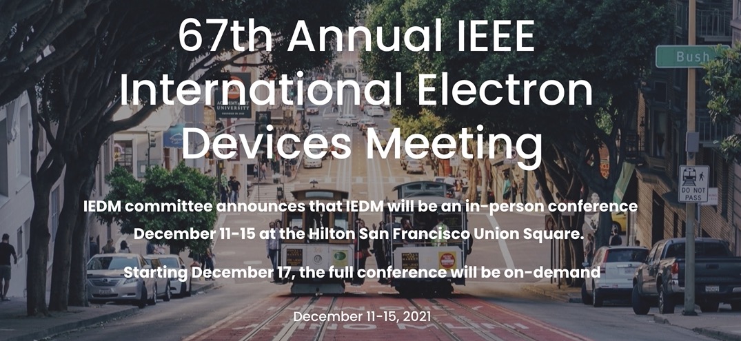
67th IEEE IEDM
Hilton San Francisco Union Square 333 O'Farrell Street, San Francisco, United StatesIEEE International Electron Devices Meeting (IEDM) is the world’s preeminent forum for reporting technological breakthroughs in the areas of semiconductor and electronic device technology, design, manufacturing, physics, and modeling. IEDM is the flagship conference for nanometer-scale CMOS transistor technology, advanced memory, displays, sensors, MEMS devices, novel quantum and nano-scale devices and phenomenology, optoelectronics, devices for… 67th IEEE IEDM
-
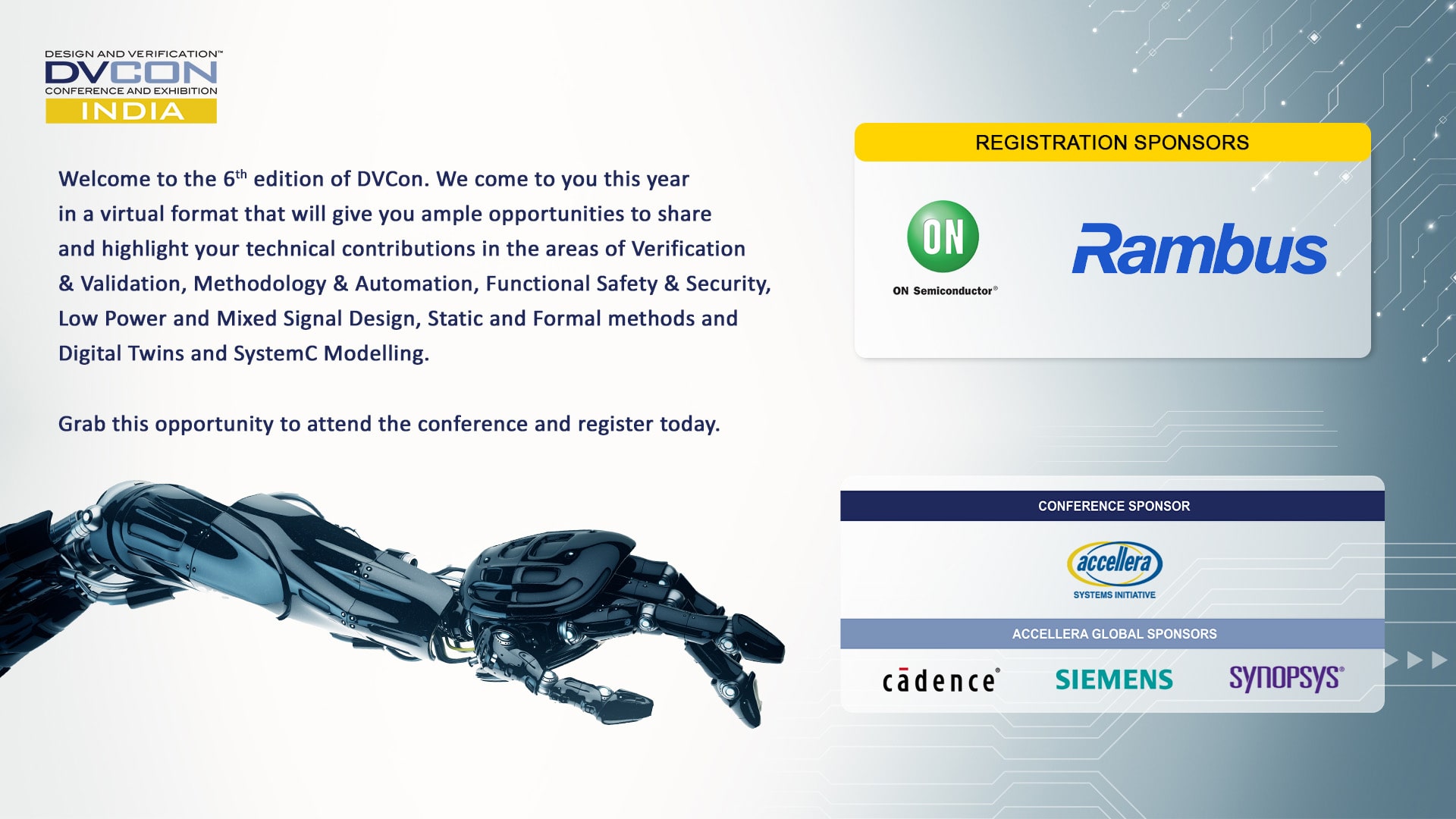
DVCON India
This conference will give you ample opportunities to share and highlight your technical contibutions in the areas of Verificaiton and Validations, Methodology & Automation, Functional Safety & Security, Low Power and Mixed Signal Design, Static and Formal methods and Digital Twins and SystemC Modeling. Kindly use this opportunity and register yourself for the conference.… DVCON India
12 events found.